- 您现在的位置:买卖IC网 > Sheet目录1200 > C8051F320DK-U (Silicon Laboratories Inc)DEV KIT FOR C8051F320/F321
�� �
�
�C8051F32x�
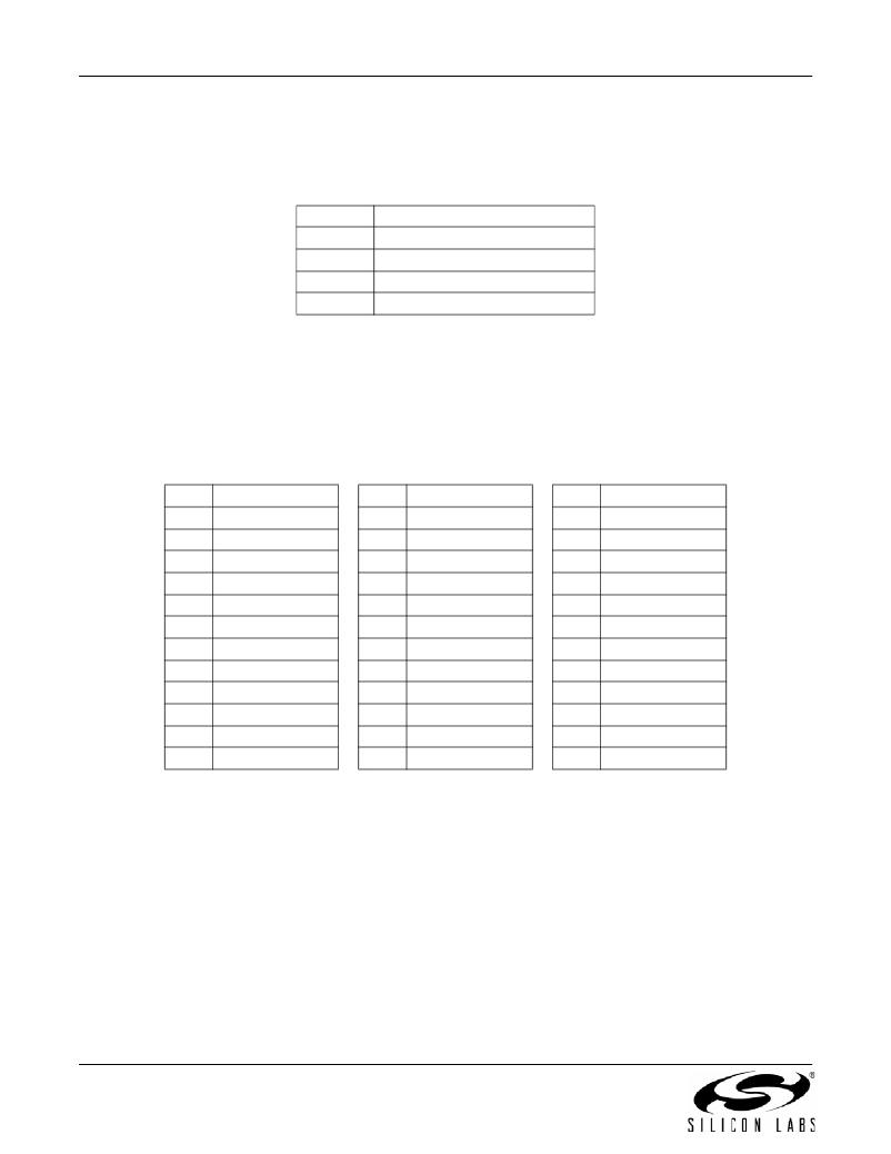
�4.3.� Universal� Serial� Bus� (USB)� Interface� (J14)�
�A� Universal� Serial� Bus� (USB)� connector� (J14)� is� provided� to� facilitate� connections� to� the� USB� interface� on� the�
�C8051F320.� Table� 2� shows� the� J14� pin� definitions.�
�Table� 2.� USB� Connector� Pin� Descriptions�
�Pin� #�
�1�
�2�
�3�
�4�
�Description�
�VBUS�
�D-�
�D+�
�GND� (Ground)�
�4.4.� Expansion� I/O� Connector� (J1)�
�The� 32-pin� Expansion� I/O� connector� J1� provides� access� to� all� signal� pins� of� the� C8051F320� device.� Pins� for� +3� V,�
�digital� ground� and� the� output� of� an� on-board� low-pass� filter� are� also� available.� A� small� through-hole� prototyping�
�area� is� also� provided.� All� I/O� signals� routed� to� connector� J1� are� also� routed� to� through-hole� connection� points�
�between� J1� and� the� prototyping� area� (see� Figure� 4� on� page� 6).� Each� connection� point� is� labeled� indicating� the�
�signal� available� at� the� connection� point.� See� Table� 3� for� a� list� of� pin� descriptions� for� J1.�
�Table� 3.� J1� Pin� Descriptions�
�Pin� #�
�1�
�2�
�3�
�4�
�5�
�6�
�7�
�8�
�9�
�10�
�11�
�12�
�Description�
�+3� VD� (+3.3� VDC)�
�PWM� Output�
�P0.0�
�P0.1�
�P0.2�
�P0.3�
�P0.4�
�P0.5�
�P0.6�
�P0.7�
�P1.0�
�P1.1�
�Pin� #�
�13�
�14�
�15�
�16�
�17�
�18�
�19�
�20�
�21�
�22�
�23�
�24�
�Description�
�P1.2�
�P1.3�
�P1.4�
�P1.5�
�P1.6�
�P1.7�
�P2.0�
�P2.1�
�P2.2�
�P2.3�
�P2.4�
�P2.5�
�Pin� #�
�25�
�26�
�27�
�28�
�29�
�30�
�31�
�32�
�Description�
�P2.6�
�P2.7�
�P3.0�
�/RST� (Reset)�
�VREGIN�
�VDD�
�VBUS�
�GND� (Ground)�
�4.5.� USB� Self-Powered� Configuration� (J2,� J11)�
�The� C8051F320� target� board� can� be� configured� as� a� self-powered� USB� device� to� take� power� from� the� USB� cable�
�instead� of� the� ac/dc� adapter� connected� at� P1.� To� configure� the� target� boards� as� a� self-powered� USB� device,�
�remove� the� shorting� block� from� J2� and� install� on� J11.� (A� shorting� block� should� only� be� installed� on� J2� or� J11,� never�
�both� at� the� same� time.)� Install� shorting� blocks� in� the� following� manner:�
�J2(ON)� &� J11(OFF)� ?� Target� Board� is� powered� from� the� ac/dc� Adapter� at� P1.�
�J2(OFF)� &� J11(ON)� ?� Target� Board� is� powered� from� the� USB� connection�
�Note:� When� the� C8051F320� target� board� is� self-powered� from� the� USB,� the� Serial� Adapter� is� not� powered� from� the�
�target� board.� The� Serial� Adapter� must� be� powered� directly� by� connecting� the� ac/dc� adapter� to� the� Serial� Adapters’�
�dc� power� jack.� Also,� the� RS232� Serial� Interface� (J5)� cannot� be� used� when� powering� the� target� board� from� the� USB.�
�8�
�Rev.� 0.9�
�发布紧急采购,3分钟左右您将得到回复。
相关PDF资料
C850-260-WHX
CIRCUIT PROT 260MA 850VIMP TBU
CAN0005WP
VARISTOR 18VDC 4A 0402
CB4-B0-24-650-121-C
CIRCUIT BREAKER 50A 4POLE 8 PIN
CBBJ159
TRS BULKHEAD RCPT STR PCB
CBBJ379
TRT BULKHEAD JACK STR PCB THREAD
CBBJ79
TRB BULKHEAD JACK STR PCB 3-LUG
CBBJR26
BNC BULKHEAD JACK INSUL R/A PCB
CBBJR29
BNC BULKHEAD JACK R/A PCB
相关代理商/技术参数
C8051F320-GQ
功能描述:8位微控制器 -MCU 16KB 10ADC USB 32P MCU Rev E RoHS:否 制造商:Silicon Labs 核心:8051 处理器系列:C8051F39x 数据总线宽度:8 bit 最大时钟频率:50 MHz 程序存储器大小:16 KB 数据 RAM 大小:1 KB 片上 ADC:Yes 工作电源电压:1.8 V to 3.6 V 工作温度范围:- 40 C to + 105 C 封装 / 箱体:QFN-20 安装风格:SMD/SMT
C8051F320-GQR
功能描述:8位微控制器 -MCU 16KB 10ADC USB 32Pin Tape and Reel RoHS:否 制造商:Silicon Labs 核心:8051 处理器系列:C8051F39x 数据总线宽度:8 bit 最大时钟频率:50 MHz 程序存储器大小:16 KB 数据 RAM 大小:1 KB 片上 ADC:Yes 工作电源电压:1.8 V to 3.6 V 工作温度范围:- 40 C to + 105 C 封装 / 箱体:QFN-20 安装风格:SMD/SMT
C8051F320R
功能描述:8位微控制器 -MCU 10 ADC 32 Pin RoHS:否 制造商:Silicon Labs 核心:8051 处理器系列:C8051F39x 数据总线宽度:8 bit 最大时钟频率:50 MHz 程序存储器大小:16 KB 数据 RAM 大小:1 KB 片上 ADC:Yes 工作电源电压:1.8 V to 3.6 V 工作温度范围:- 40 C to + 105 C 封装 / 箱体:QFN-20 安装风格:SMD/SMT
C8051F320-TB
功能描述:插座和适配器 With C8051F320 MCU RoHS:否 制造商:Silicon Labs 产品:Adapter 用于:EM35x
C8051F320-TB-K
功能描述:BOARD PROTOTYPING W/C8051F320 制造商:silicon labs 系列:- 零件状态:在售 板类型:评估平台 类型:MCU 8-位 核心处理器:8051 操作系统:- 平台:- 配套使用产品/相关产品:C8051F32x 安装类型:固定 内容:板 标准包装:1
C8051F321
功能描述:8位微控制器 -MCU 16KB 10ADC RoHS:否 制造商:Silicon Labs 核心:8051 处理器系列:C8051F39x 数据总线宽度:8 bit 最大时钟频率:50 MHz 程序存储器大小:16 KB 数据 RAM 大小:1 KB 片上 ADC:Yes 工作电源电压:1.8 V to 3.6 V 工作温度范围:- 40 C to + 105 C 封装 / 箱体:QFN-20 安装风格:SMD/SMT
C8051F321-GM
功能描述:8位微控制器 -MCU 16KB 10ADC USB 28P MCU REV E RoHS:否 制造商:Silicon Labs 核心:8051 处理器系列:C8051F39x 数据总线宽度:8 bit 最大时钟频率:50 MHz 程序存储器大小:16 KB 数据 RAM 大小:1 KB 片上 ADC:Yes 工作电源电压:1.8 V to 3.6 V 工作温度范围:- 40 C to + 105 C 封装 / 箱体:QFN-20 安装风格:SMD/SMT
C8051F321-GMR
功能描述:8位微控制器 -MCU 16KB 10ADC USB 28P MCU REV E RoHS:否 制造商:Silicon Labs 核心:8051 处理器系列:C8051F39x 数据总线宽度:8 bit 最大时钟频率:50 MHz 程序存储器大小:16 KB 数据 RAM 大小:1 KB 片上 ADC:Yes 工作电源电压:1.8 V to 3.6 V 工作温度范围:- 40 C to + 105 C 封装 / 箱体:QFN-20 安装风格:SMD/SMT